    |
Nanometer-sized beam with a glass capillary
|
Generally, glass does not conduct electricity.
Static electricity on glass tends to build up due to friction.
This static is difficult to eliminate.
So, when using an ion beam, glass is normally avoided in any place where the beam passes.
There have been very few trials to control the direction and the size of an ion beam
with glass.
We have introduced thin glass tube with a fine beam exit
as a tool for We are planning to use not only positive/negative ions but also elementally particles such as positrons and others. In this web site, we will introduce our experiments so far. |
|
|
||
|
(Tokihiro Ikeda#), Yasuyuki Kanai, Takao M. Kojima, |
| Tomohiro Kobayashi, and Yasunori Yamazaki, (Walter Meissl, Yoshio Iwai) |
| Atomic Physics Laboratory, RIKEN |
|
Masamitsu Hoshino |
| Sophia University |
|
Nagayasu Oshima |
| AIST |
|
Tadashi Narusawa, (Takuya Nebiki) |
| Kochi University of Technology |
|
Amine Cassimi, Laurent Maunoury, Henning Lebius, |
|
Bruno Manil, and Bernd Huber |
| CIMAP |
|
(Tomoko Muranaka) |
| CEA-Saclay |
|
* (Persons) left.
|
Introduction
| When a highly charged ion (HCI) with a kinetic energy ranging from keV to several tens keV collides with a surface, the ion cannot penetrate deeply but affects only the surface via its large potential energy. We call the HCI in this kinetic energy region "slow" HCI. | |||
| An HCI's potential energy is controllable by selecting the ion and the charge state. For example, an Ar8+ ion has a potential energy of about 600 eV. In the case of U92+, it is approximately 800 keV, which is about 1.6 times as large as an electron mass. | |||
| Slow HCIs have the high ability to modify surfaces and cause efficient sputtering without damaging the substrate. For example, the F-Si bond direction of a Si(001)-F surface can be reconstructed from the three-dimensional momentum distribution of F+ ions desorbed by slow HCIs1); i.e., a stereochemical analysis can be done with slow HCIs. It was also found a single HCI induces a nanometer dot on graphite2-4), Al2O3 2) , gold 5), CaF2 6-7) and SiO2 8) surfaces. | |||
| Once a microbeam is available, these functions specific to slow HCIs can be used to realize, e.g., micropatterning of nanodots and element-sensitive microimaging. | |||
| Conventionally, collimators and magnetic and/or electric lenses have been employed to produce microbeams. When a collimator is used, we will be concerned about not only the drastic reduction of the beam intensity but also the charge transfer and the energy loss of the ions due to the touching the inner wall. If you add the lenses, good emittance of the initial beam is also required. | |||
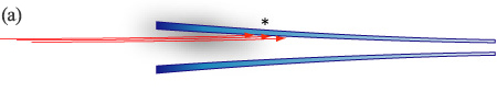
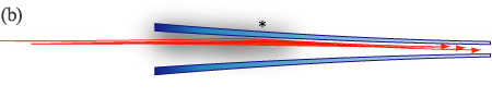
| We have developed the method to realize a nano-meter sized beam with increased particle density based on the self-organized charge-up on the insulator surface of the inner wall of glass capillaries9-14). This method does not always need a collimator nor an electric or magnetic lens. The following figures explain the model of the focusing. In the pictures, the blue regions correspond to the cross-section of an insulator tube. The ion beam enters from the left side of the capillary and exits from the right side. The inner diameter of the inlet is larger than that of the outlet (tapered shape). | |||
|
|
|||
| When the surface of the inner wall is uncharged, the ions arriving at the point (*) on the wall will be stopped there. That point will then become gradually charged-up due to the ions' charge (Fig.(a)). | |||
|
|
|||
| When the accumulated charge gets large enough to prevent the following incident ions from touching the inner wall, the ions travel more or less parallel to the wall (Fig.(b)), and guiding is realized. | |||
| The reflection on the inner wall does not always require an exact angle between the beam axis and the surface. This means that transmission can take place even if the beam axis has an angle with respect to the capillary axis, that is, guiding effect. We have to emphasize the difference from transportation using the active potentials which we supply and modify artificially. In this sense, the potential from a self-organized charge-up region can be regarded as passive. Because the latter potential becomes into an equilibrium by degrees as if the potential guided the beam in a certain direction. In the following section, we will overview the history of our research of HCI's and some types of capillaries. | |||
| References | |||
|
1) |
N. Okabayashi, K. Komaki, and Y. Yamazaki, "Secondary ion emission from a water and fluorine adsorbed Si(1 0 0) surface irradiated with electrons and highly charged ions", Nucl. Instr. and Meth. B 205, 725 (2003).[html] | ||
|
2) |
I. C. Gebeshuber, |
||
|
3) |
N. Nakamura, M. Terada, Y. Nakai, Y. Kanai, S. Ohtani, K. Komaki, and Y. Yamazaki, "SPM observation of nano-dots induced by slow highly charged ions", Nucl. Instr. and Meth. B 232, 261 (2005). [html] | ||
|
4) |
M. Terada, N. Nakamura, Y. Nakai, Y. Kanai, S. Ohtani, K. Komaki, and Y. Yamazaki, "Observation of an HCI-induced nano-dot on an HOPG surface with STM and AFM", Nucl. Instr. and Meth. B 235, 452 (2005). [html] | ||
|
5) |
J. M. Pomeroy, A. C. Perrella, H. Grube, and J. D. Gillaspy, "Gold nanostructures created by highly charged ions", Phys. Rev. B 75, 241409 (2007). [html] | ||
| 6) | A.S. El-Said, W. Meissl, M.C. Simon, J.R. Crespo López-Urrutia, C. Lemell, J. Burgdörfer, I.C. Gebeshuber, HP. Winter, J. Ullrich, C. Trautmann, M. Toulemonde, and F. Aumayr, "Potential energy threshold for nano-hillock formation by impact of slow highly charged ions on a CaF2(1 1 1) surface", Nucl. Instr. and Meth. B 258, 167 (2007). [html] | ||
| 7) | C. Lemell, A.S. El-Said, W. Meissl, I.C. Gebeshuber, C. Trautmann, M. Toulemonde, J. Burgdörfer, and F. Aumayr, "On the nano-hillock formation induced by slow highly charged ions on insulator surfaces", Solid-State Electronics 51, 1398 (2007). [html] | ||
| 8) | Masahide Tona, Hirofumi Watanabe, Satoshi Takahashi, Nobuyuki Nakamura, Nobuo Yoshiyasu, Makoto Sakurai, Toshifumi Terui, Shinro Mashiko, Chikashi Yamada, and Shunsuke Ohtani, "Nano-crater formation on a Si(1 1 1)-(7 x 7) surface by slow highly charged ion-impact", Surface Science 601, 723 (2007). [html] | ||
|
* * * |
|||
|
9) |
T. Ikeda, Y. Kanai, T. M. Kojima, Y. Iwai, T. Kambara, M. Hoshino, T. Nebiki, T. Narusawa, and Y. Yamazaki, "Production of a microbeam of slow highly charged ions with a tapered glass capillary", Appl. Phys. Lett. 89, 163502 (2006).[html] | ||
| 10) | T Ikeda, T M Kojima, Y Iwai, Y Kanai, T Kambara, T Nebiki, T Narusawa, and Y Yamazaki, "Production of a nm sized slow HCI beam with a guiding effect", Journal of Physics: Conference Series 58 68 (2007).[html] | ||
|
11) |
T Ikeda, Y Kanai, T M Kojima, Y Iwai, Y Kanazawa, M Hoshino, T Kobayashi, G P Pokhil, and Y Yamazaki, "Focusing of charged particle beams with various glass-made optics", Journal of Physics: Conference Series 88 012031 (2007).[html] | ||
| 12) | T. Ikeda, Y. Kanai, T. M. Kojima, Y. Iwai, and Y. Yamazaki, "Production of nm sized highly charged ion beam based on guiding effect of insulator capillaries", Radiation Chemistry 83, 21 (2007).[in Japanese][html] | ||
| 13) | T. Ikeda and N. Oshima, "Production of high-quality beam of highly charged ions", Journal of Plasma and Fusion Research 83, 8, 690 (2007).[in Japanese][html] | ||
|
14) |
T. Ikeda, Y. Iwai, Y. Kanai, T. M. Kojima, T. Nebiki, T. Narusawa, and Y. Yamazaki, "Production and application of a nano-sized beam of highly charged ion in a keV region", J. Vac. Soc. Jpn. 50, 9, 569 (2007).[in Japanese][html] | ||
Metallic capillaries, Insulator capillaries, and slow HCI
| The interaction between HCI beam and an insulator surface of the inner wall of nano-capillaries was studied for the first time by Yamazaki et al.15,16), who used multitudes of nano-capillaries in a thin insulator foil. This type of foil is called an insulator multi-capillary foil. | ||||
| Then, instead of insulator, metallic multi-capillary foils were introduced. This type of foil has been used as a tool for extracting hollow atoms (ions) into vacuum. This method enables us to the investigate the nature of hollow atoms (ions)16-26). After that, insulator multi-capillary foil was focused again by Stolterfoht et al.27-40) and Kanai et al.35,36). They reported the guiding effect for HCIs with a keV energy based on self-organized charge-up process using a polyethylene terephthalate (PET) foil. | ||||
| Independently, a tapered glass capillary with a length of several cm was introduced for focusing MeV proton or He ion beams down to micro-meter or nano-meter size 41,42 ,*). This was not a multitude of capillaries. So it is called a single (tapered) capillary. | ||||
| The tapered glass capillary shown here has been developed for the first time in RIKEN to have the advantages of both the guiding effect with the insulator multi-capillary foil and the focusing effect with the tapered single glass capillary. We have proven " the method of producing microbeam based on the self-organized charge-up with a tapered glass capillary". The new capillaries made in RIKEN have already been used and showed results with slow HCI's in CIMAP (Ciril)43). | ||||
| As well as single capillaries, the study of the insulator multi-capillary foil shows rapid progress with PET, SiO244,45)and Al2O346-49). Also computer simulations explaining the phenomena have reported remarkable advances50-54). In recent international conferences, there have been more and more reports with the keywords "guiding" and "capillary". Clearly the phenomena of "self-organized charge-up" are getting more popular55). | ||||
|
*) |
In this site, we treat the glass capillary focusing for only slow HCI beams not for MeV beams. Although the focusing for MeV beams (with intensity of nA ) can be seen elsewhere, we would like to emphasize the following different points; (1) For slow HCI, the time (several seconds to several tens seconds) to establish the self-organize charge-up distribution can seen. But for a MeV beam, the transmission takes place immediately. (2) For slow HCI, the guiding effect can be seen even if the capillary axis is slightly different from the beam axis, whereas for a MeV beam, the transmission reduces drastically. |
|||
| In the following sections, we will report our experiments to show that a tapered single glass capillary can be used as a tool to produce a microbeam or a nanobeam. | ||||
| References 15-55) | ||||
Glass capillary
| manufacture |
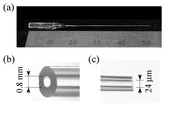
The glass capillaries we have employed were made of borosilicate. The tapered capillary was prepared by heating a straight glass tube, whose dimension is 2 mmf in outer diameter, 0.8 mmf in inner diameter and 90 mm in length, and then stretched by pulling both ends with a constant force. |
|||||||||||||||||
| composition | This glass is typically composed of SiO2: 80.9 %, Al2O3: 2.3 %, B2O3: 12.7 %, Na2O: 4.0 %, K2O: 0.04 %. Its density of 2.23, which is almost the same as silica glass, is hard enough to prevent the slow HCI beam from penetrating a capillary wall with a thickness of more than 1 mm under the condition of oblique incidence. | |||||||||||||||||
| thermal expansion | The coefficient of linear thermal expansion is 32×10-7/oC, which is the second smallest after that of silica glass. Therefore, borosilicate has been used the glass instruments in chemical and physical experiments as well as silica glass. However, the method of the forming is easier than silica glass because of the following reasons. | |||||||||||||||||
| flow resistance |
Glass has been formed and shaped by heating since ancient times, it is well
known that heating decreases
the flow resistance of glass.
There are some critical temperatures corresponding to the typical phenomena. The temperatures
for borosilicate are listed below.
Where poise = dyn.s/cm2 = 0.1Pa.s is a unit of flow resistance.
|
|||||||||||||||||
| softening temperature | It might be hard to imagine how the glass flows from the poise numbers. There is another expression for the Softening Point, i.e., the temperature when a glass fiber whose dimension is from 0.55 to 0.75 mmf in diameter and 229 mm in length is put at the center of an electric heating furnace, is heated by 10o/min and then flows down by gravity with the velocity of 1 mm/min56). By the way, starch syrup has a flow resistance of 105 - 106 poise, depending on temperature. A substance with a flow resistance beyond 1013 poise can be regarded as a solid. | |||||||||||||||||
| forming | Generally glass can be formed and shaped with a flow resistance of 104 - 108 poise. However, the corresponding temperature depends on the glass type. We have to take into account the heating method according to the glass type. In order to make the glass needles for microinjection to a living cell or the glass electrodes for patch clamping to contact the cell membrane to measure cell potential, a tool to manufacture the glass tube (called a puller) is commercially available. In the case of a tube made from silica glass, whose softening temperature is more than 1500oC, the puller consists of a laser for heating. On the other hand, in the case of lead glass, whose softening temperature is about 600oC, there sometimes remains a thin thread between both sides after the heating up has stopped. | |||||||||||||||||
| shape control | We have fabricated the glass capillary by heating up a glass tube with a heater coil in atmosphere keeping the tube at the middle of the coil. In order to make a tapered glass capillary 5 cm-long, borosilicate would be the best glass type in terms of (1) its softening temperature and (2) the cooling velocity of the glass itself after the heating up. The taper angle of the capillary related to the length governs the characteristics of the beam transmission. The temperature of the heater and the force of pulling are the main parameters to control the taper angle. | |||||||||||||||||
| nm sized | This material can also provide an outlet in the order of 100 nmf to realize a nano-meter sized beam. As seen in the photograph here, the outlet of inner diameter of 80 nmf has been obtained. | 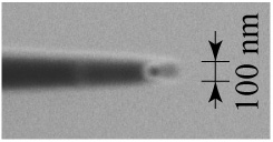 |
||||||||||||||||
| Reference | ||||||||||||||||||
|
56) |
Yasukazu Hasegawa,
Uchida Roukakuho Publishing Co. Ltd. (1993) ISBN:4753651177. [in Japanese]
and Tsutomu Minami, Sangyo Tosyo (1993) ISBN:4782835515. [in Japanese] |
|||||||||||||||||
Experiments
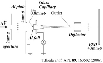
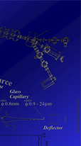
| Setup | The experiments for confirming the guiding effect and producing the nano-sized beam have been performed in RIKEN. An ion beam was extracted from a 14.5 GHz Caprice electron cyclotron resonance ion source, and then transported to an experimental chamber (Fig.below) with a vacuum of about 4x10⁻⁵Pa. | ||
|
|
|||
| An Ar8+ion beam of 8 keV was then collimated by a 2 mmf aperture and injected to a tapered glass capillary, where the divergence of the beam after the aperture was at most +/- 3.3 mrad. Figure (a) shows the whole glass capillary of about 50 mm-length. Figure (b) is a photograph of the inlet with the outer diameter of 2 mmf and inner diameter of 0.8 mmf. And the outlet whose inner diameter of 24 mmf is shown in Fig.(c). | |||
|
|
|||
| The extracted beam from the capillary outlet was detected by a position sensitive detector (PSD) with a sensitive area of 40 mmf consisting of a stack of multichannel plates and wedge-and-strip-type anode. A deflector was installed between the capillary and the PSD for charge-state analysis. As seen in the figure of the setup, the edge around the capillary inlet was covered with an Al foil with a 0.8 mmf hole to avoid macroscopic charge-up of the entrance surface of the capillary. The additional ring with the diameter of 6 mmf prevented the direct beam arriving at the PSD. It was also used as a monitor of the incoming ion current. | |||
| The monitored current was corrected according to the assumption of the secondary electron yield of approximately 7e-/Ar8+ for several keV Ar8+ ion from Al surface57). As the shape of the incident beam spot at the Al foil was known, the real current entering the inlet was evaluated from the corrected current at the Al foil. | |||
| Reference | |||
|
57) |
A. Arnau, F. Aumayr, P. M. Echenique, M. Grether, W. Heiland, J. Limburg, R. Morgenstern, P. Roncin, S. Schippers, R. Schuch, N. Stolterfoht, P. Varga, T. J. M. Zouros, and H. P. Winter, Surface Science Reports 27, 113 (1997). [html] | ||
Intensity and Focusing effect
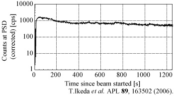
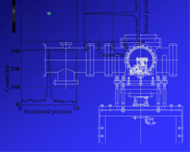
| The following figure shows the transmitted ion intensity as a function of time for the glass capillary injected with an 8 keV Ar8+ ion beam of 0.2 pA9). | |||
|
|
|||
| This plot was obtained with a capillary whose inner diameter of the outlet was 24 mmf. The horizontal axis is the time since the irradiation started. The vertical axis corresponds to the counts per second at the PSD, which was already corrected with the detection efficiency of 50 %. It is seen that the transmission current had been kept for more than 1200 s, where the incident beam was also constant with a stability at most 10 %. (The other data for different initial current or outlet size are shown elsewhere7).) | |||
| The peak count was found to be 1600 cps. The beam density at the outlet increased by approximately 10 times compared with that at the inlet, taking into account the ratio between the areas of outlet and inlet and the ratio between the numbers of ions at the outlet and inlet. We confirmed the focusing effect, and we call the increase by 10 times in the density Enhancement Factor (E.F.) = 10. | |||
| As it took about 40 s to maximize the transmitted current, the self-organized charge-up could have been established within this 40 s. In order to confirm that the extracted ions never touched the inner wall of the capillary at the reflection, the following experiments were carried out. | |||
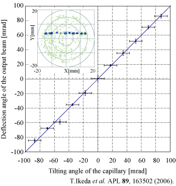
Guiding effect
| The upper left inset of the following figure shows the position of the transmitted beam on the PSD when the capillary was tilted horizontally around the entrance of the capillary by -5o(=-87 mrad) to +5o with a step of 1o relative to the incident beam axis. The corresponding spots of the transmitted beam were observed on the PSD9). | |||
|
|
|||
| The horizontal axis in the above plot is the tilting angle of the capillary and the vertical axis is the deflected angle of the output beam which was reconstructed from the position of the spots on PSD. Taking into account that the divergence of the initial beam was about +/- 3 mrad, and the geometrical limit of the capillary shape for the straight beam is about +/- 0.5o (=+/- 8 mrad), the data points on the line y=x means that the beam was bent due to the reflection of the inner wall, and was then extracted in the same direction as the capillary axis. | |||
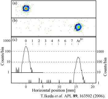
Charge transfer
| The charge-state distribution of the transmitted ions was measured by biasing the deflector. The following Fig.(a) shows the 2D spot at the PSD without the deflector bias, while Fig.(b) shows the spot with the bias. The peaks in Fig.(c) show the projected beam profiles corresponding to Figs.(a) and (b) with a scale of the charge states from neutral to +8 9). | |||
|
|
|||
| In the region corresponding to charge-changed components, there were no peaks. The fraction of the ions in other charge states, including the background events, was found to be less than 1 % for the all events in the region of all charge states, which corresponds to the region of Fig.(b). If the transmitted ions touched the inner wall, the Ar8+ ions would capture some electrons from the wall surface and then change themselves to the lower charge state, considering their low kinetic energy. Our data shows that the transmitted ions did not change their charge state. The Ar8+ ions must have not touched the inner wall of the capillary. | |||
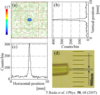
Nano sized beam
| The above reports were for the glass capillary having the outlet of 24 mmf. In order to make a manometer sized beam, we prepared a capillary with the outlet of 900 nmf for the transmission experiments. An Ar8+ beam with the energy of 64 keV was employed. The following figure (a) shows the extracted beam profile on the PSD. Figs.(b) and (c) are the projected profiles on the vertical and horizontal axes, respectively10). | |||
|
|
|||
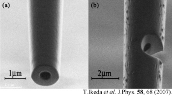
| The spot had vertical and horizontal widths (FWHM) of 0.3 mm and 0.4 mm, respectively. The corresponding beam divergences are +/- 2 mrad and +/- 3 mrad, respectively. The figure (d) is a photograph of the outlet. The extracted beam with the energy of 64 keV cannot penetrate the wall of the capillary. The extracted beam size of 900 nmf or less was realized. | |||
| The capillary with the outlet of 900 nmf used in above experiment was manufactured under an optical microscope. However, it could be close to the limit size for optical microscope. In order to fabricate and observe the smaller structures around the capillary outlet, a focused ion beam (FIB), which is commercially available, has been employed. | |||
|
|
|||
| Figure (a) is a photograph of a manufactured outlet with an inner diameter of 500 nmf. The FIB uses a Ga+ beam accelerated by 40 kV and focused to approximately 20 nmf. Various shapes, for example, Fig.(b), can be realized with an adjustment of scan direction, the ratio of the interlace and beam intensity to avoid the charge-up of the capillary, according to the size of the capillary outlet 10). | |||
Summary
| It is essential to know the target position on the sample to be irradiated when using a nano-/micro-meter sized beam. Therefore, it is one of the advantages to see the outlet of the beam exit easily. It may be necessary to locate the sample close to the capillary exit. In this case, it is also useful to avoid any electric or magnetic field for the beam focusing. Moreover, the guiding effect by 1 or 2o is helpful to move the beam spot. In practical use, moving the beam is sometimes more convenient than changing the sample position. | |||
| The aim of this study is not only the development of the method to produce nano-meter sized beams with glass capillaries but also the understanding of the interaction between charged particles and insulator surfaces. | |||
| This work was partly supported by a Grant-in-Aid for Scientific Research ( No. 17654079, No. 20510119 ) from the Ministry of Education, Culture, Sports, Science, and Technology, Japan and a Grant of "Developments and Applications of Exotic Quantum Beams" and a FY2008 Incentive Research Grant from RIKEN. | |||
| Address | ||
| |
Atomic Physics Laboratory, RIKEN 2-1 Hirosawa, Wako, Saitama 351-0198, Japan Atomic Physics Laboratory, RIKEN (Main Research Building, 6F) TEL. +81-48-462-1111 FAX. +81-48-462-4644 (direct) |
|
| Access | ||
| To RIKEN Headquarters, Wako Institute | ||
| Layout of facilities in Wako Institute | ||
| Modified, 6/Feb/2013 by |
| Back |
Copyright (c) 2007-2013 Atomic Physics Laboratory, RIKEN. All rights reserved. |